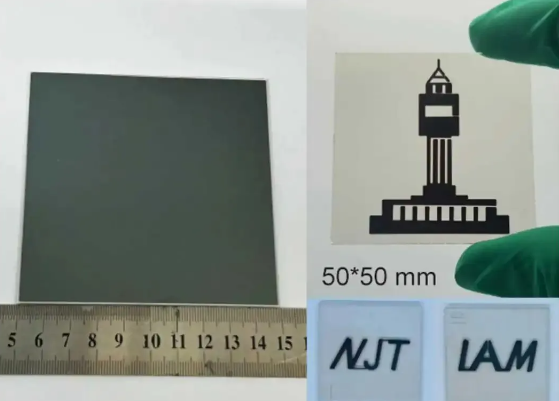
According to media reports from 163.com on November 2nd, a research team from Nanjing Tech University has successfully developed perovskite photovoltaic devices with an area of 0.066 square centimeters using a “full vacuum thermal evaporation” technique.
These devices have achieved a remarkable power conversion efficiency (PCE) of 25.19%.
Furthermore, the devices demonstrated excellent stability, maintaining over 95% of their initial performance after more than 1000 hours of continuous operation.
The team also fabricated 1-square-centimeter devices using the same method, achieving a PCE of 23.38%, indicating strong potential for industrial application.
These findings have been published in the prestigious international journal “Nature Photonics.”
Currently, solution-based methods such as spin coating and slot-die coating are widely adopted in laboratories worldwide for the fabrication of perovskite photovoltaic devices.
Xu Yutian, a doctoral student at Nanjing Tech University and the paper’s first author, pointed out that these prevalent methods often involve toxic solvents like N,N-dimethylformamide (DMF) and dimethyl sulfoxide (DMSO).
These chemicals pose potential risks to health and the environment, and their use also limits the scalability of production for large-scale manufacturing.
Professor Guo Qingxun from Nanjing Tech University, the corresponding author of the paper, explained that the “full vacuum thermal evaporation” technique employed by the team is analogous to “vapor deposition” of thin films in a vacuum environment.
This process involves heating the precursor materials until they vaporize at the molecular or atomic level and then deposit onto a substrate, forming a uniform and dense film.
This solvent-free approach offers precise process control and results in high-quality films, making it an ideal pathway for transitioning high-performance perovskite photovoltaic devices from the laboratory to industrial production.
Beyond achieving uniform film formation, a key challenge the team faced was further enhancing the power conversion efficiency.
Professor Chen Yonghua from Nanjing Tech University, a co-corresponding author, stated that the team innovatively proposed a “reverse layer-by-layer” deposition strategy.
He eloquently described it as, “Traditional methods are like laying ‘bricks’ first and then pouring ‘cement,’ while we reversed this order, depositing the ‘cement’ before the ‘bricks’.”
This sequential deposition, combined with self-assembly molecules, effectively promotes the reaction and diffusion between solid-state precursors during subsequent annealing, leading to the “growth” of high-quality perovskite crystalline thin films.
Leveraging these technological breakthroughs, the team has not only overcome efficiency bottlenecks in perovskite photovoltaic devices, boosting the efficiency of small-area cells to 25.19%, but also significantly improved the operational stability of the devices.
Academician Huang Wei from the Chinese Academy of Sciences and a co-corresponding author of the paper summarized: “This achievement not only breaks the world record for all-vacuum thermal evaporated perovskite solar cells but also lays a solid scientific foundation for future process optimization, performance enhancement, and the large-scale manufacturing of efficient, stable, and environmentally friendly perovskite photovoltaic devices.”

